What are the requirements for high precision of PCB?
PCB high precision is not a simple thing, it requires a higher standard for enterprise equipment and operator experience, and also it's an important problem in production technology. Today we are going to talk about, PCB board of high precision we need to have what conditions?
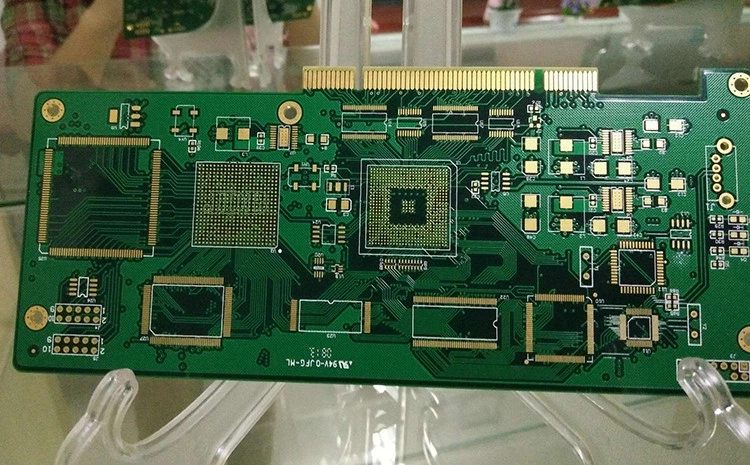
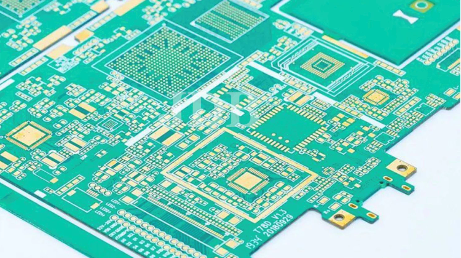
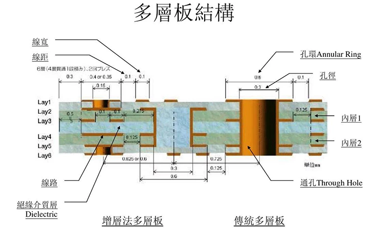
Circuit board high precision refers to the use of fine line width/spacing, small hole, narrow ring width (or ring width) and buried, blind hole and other technologies to achieve high density. And high precision refers to "thin, small, narrow, thin" results will inevitably bring high precision requirements, take line width as an example: 0.20mm line width, according to the provisions of the production of 0.16 ~ 0.24mm qualified, the error is (0.20 soil 0.04) mm; And 0.10mm line width, the same error is (0.1±0.02) mm, obviously the latter accuracy increased by 1 times, and so on is not difficult to understand, so high precision requirements are no longer discussed separately. But it is a prominent problem in production technology.
Fine wire technology
In the future, the high litichip line width/pitch will vary from 0.20mm to 0.13mm to 0.08mm to 0.005mm to meet SMT and Mulitichip Package (MCP) requirements. Therefore, the following technologies are required.
(1) substrate
Thin or ultra-thin copper foil (< 18um) substrates and fine surface treatment techniques are used.
(2) process
Thin and good quality dry film can reduce linewidth distortion and defect by using thin dry film and wet film. Wet film can fill small air gap, increase interface adhesion, improve wire integrity and accuracy.
③ Electrodeposition of photoresist film
An electro-deposited Photoresist (ED) is used. Its thickness can be controlled in the range of 5 ~ 30 / um, which can produce more perfect fine wire, especially suitable for small ring width, ringless width and whole plate plating. At present, there are more than 10 ED production lines in the world.
(4) parallel light exposure technology
Using parallel light exposure technology. Because parallel light exposure can overcome the influence of the line width variation caused by the slanting rays of the "point" light source, fine wire with precise line width and smooth edge can be obtained. But parallel exposure equipment is expensive, high investment, and requires a high degree of cleanliness in the environment.
⑤ Automatic optical detection technology
Automatic optical detection technology is adopted. This technology has become a necessary means of inspection in the production of fine wire, and is being rapidly popularized, applied and developed.
The above is the specific requirements of PCB circuit board high precision, RUNTEK has mastered these conditions and technology for a long time, so we can achieve customers' high requirements for circuit board.