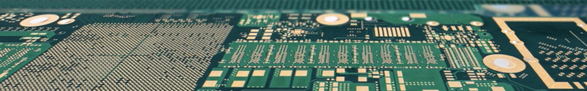
Process Capability
| Surface Finishes |
| Electroless Nickel Immersion Gold (ENIG) |
| Hot Air Solder Level (HASL, Lead and Lead‐free) |
| OSP, Immersion Tin,Immersion Silver, ENEPIG |
| Gold Fingers, Flash Gold, Full Body Hard Gold, Wire Bondable Gold |
| Selective and Multiple Surface Finishes, Carbon Ink, Peelable SM |
| Capability | Standard | Advanced |
| Line width space | 2.36/2.36mil | 2.0/2.0mil |
| Max Copper foil thickness | 2oz | 4oz |
| Min. via hole size | Min:0.2mm | Min:0.15mm |
| Min. blind hole size | Min:0.1mm | Min:0.05mm |
| Minimum semi-metallized hole | Min:0.45mm | Min:0.40mm |
| Buried hole | 4-16 layer | 24 layer |
| Max production borad size | 520mmX620mm | 540mmX640mm |
| Max Aspect ratio | 8:01 | 10:01 |
| line width space | ±20% | ±10% |
| Pth Aperture size | ±3mil | ±2mil |
| NPth Aperture size | ±2mil | ±1.5mil |
| Hole location Accuracy | ±3mil | ±2mil |
| Distance from the center of the hole to the center of the hole | ±4mil | ±3mil |
| Hole to Edge Precision | ±3mil | ±2mil |
| Layer to layer registration | ±4mil | ±3mil |
| Shape Size tolerance | ±4mil | ±3mil |
| Impedance tolerances | ±10% | ±8% |
| Min.Solder Mask Dam Width | Green Oil:3mil | Green Oil:2.5mil |
| Other:4.5mil | Other:4mil | |
| S/M Registration | ±1.5mil | ±1.2mil |
| Min. SMT/QFP Pitch | 10mil | NA |
| Min. BGA Pitch | 12mil | NA |
| Max. Test Points/Board(Universal ET) | Bed of Nail Test:16000 | NA |
| Flying Probe Test:1-∞ | ||
| v-cut Depthing | ±4mil | ±3mil |
| v-cut Angel | 20°、30°、45° | NA |
| v-cut precision | ±4mil | ±3mil |
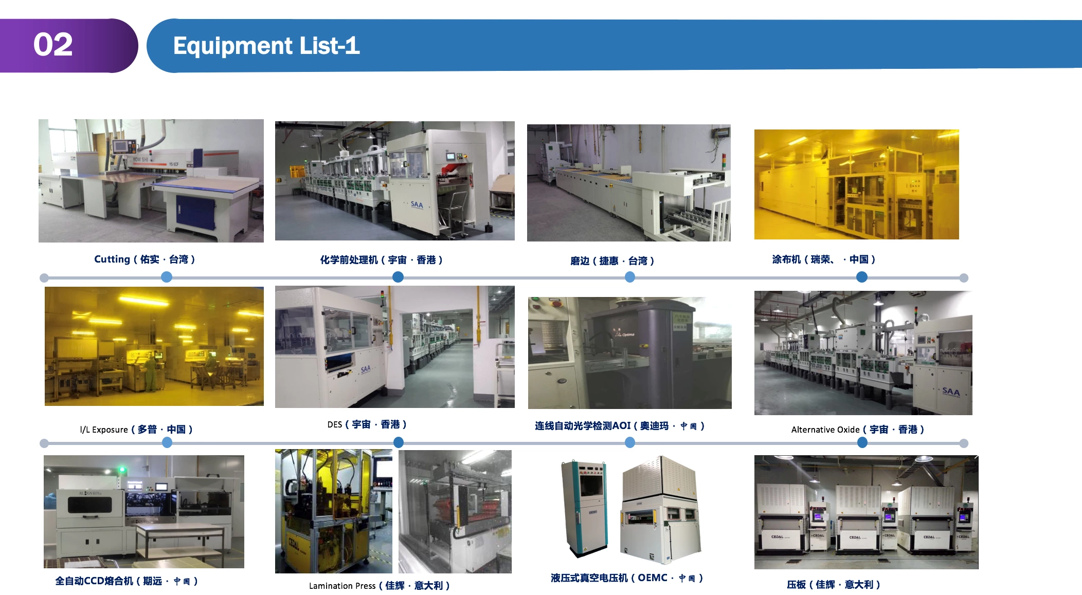
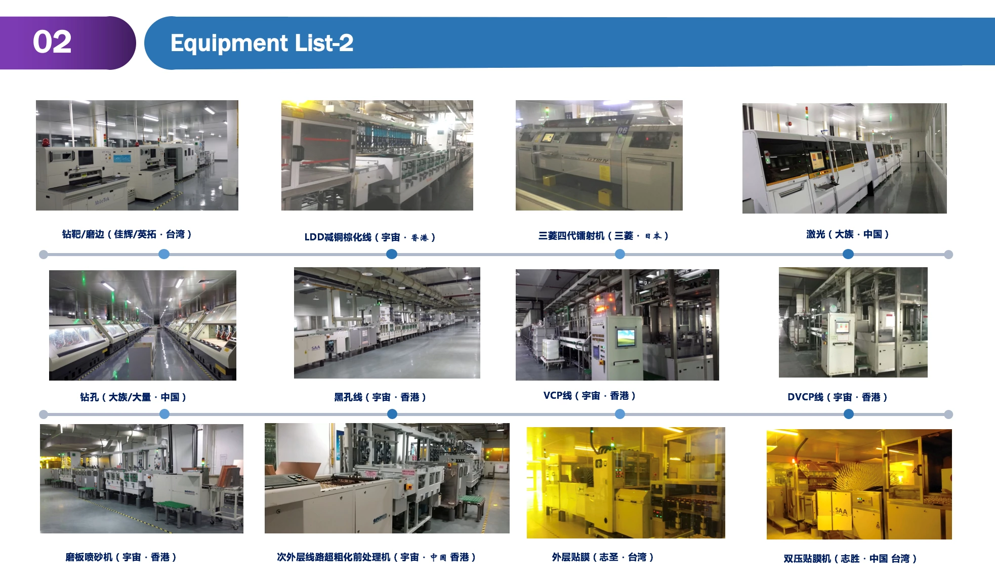
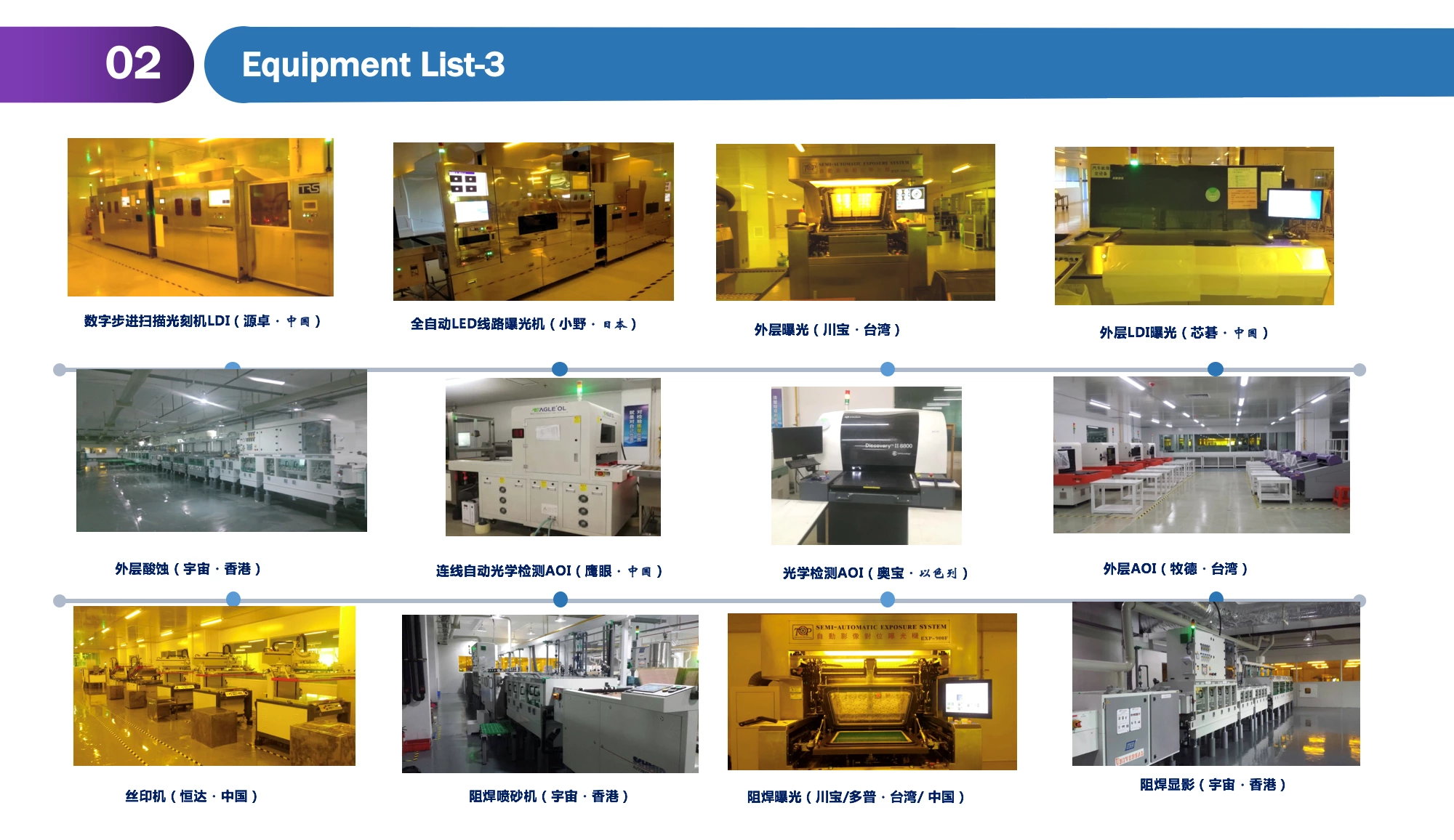
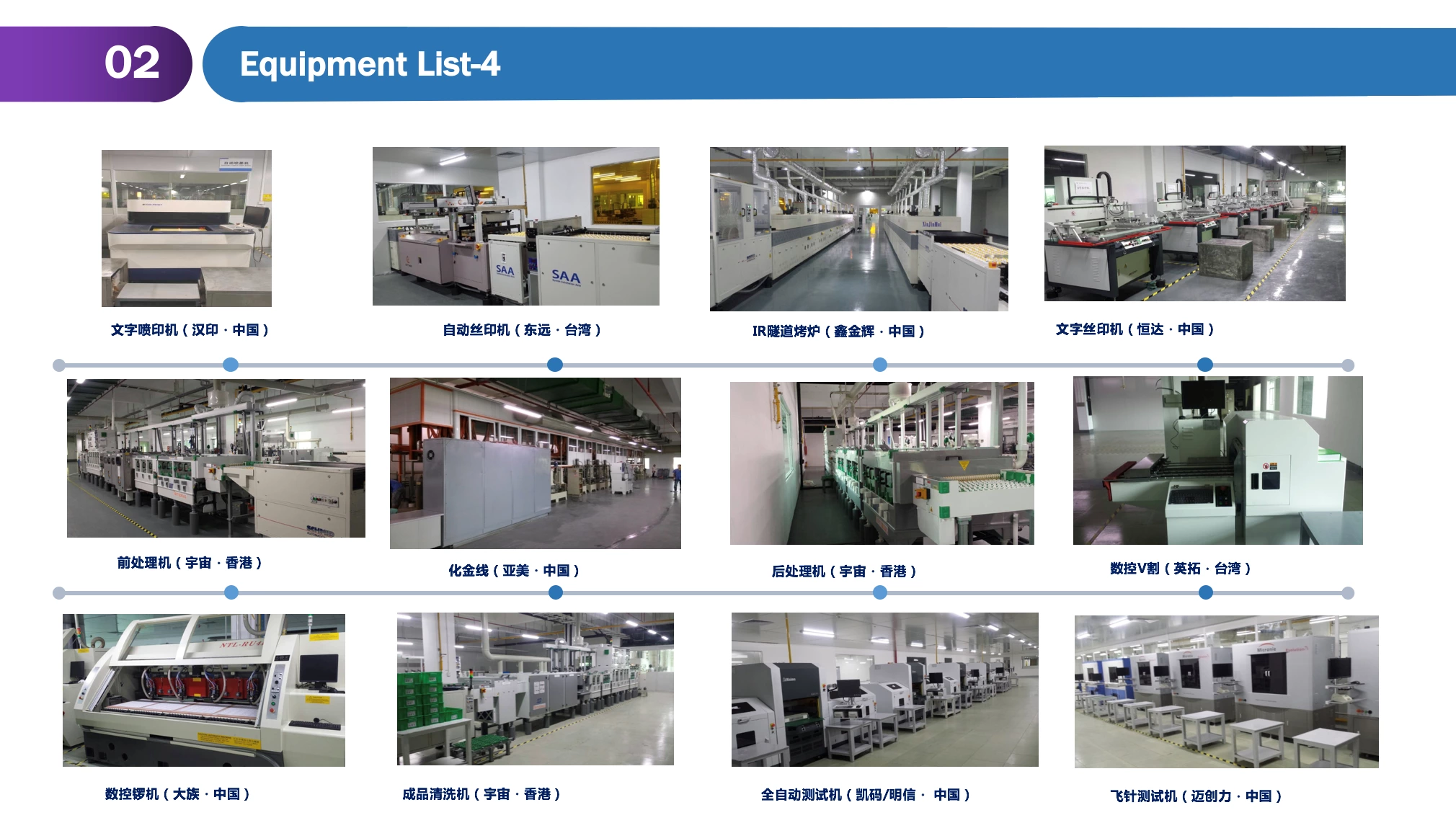
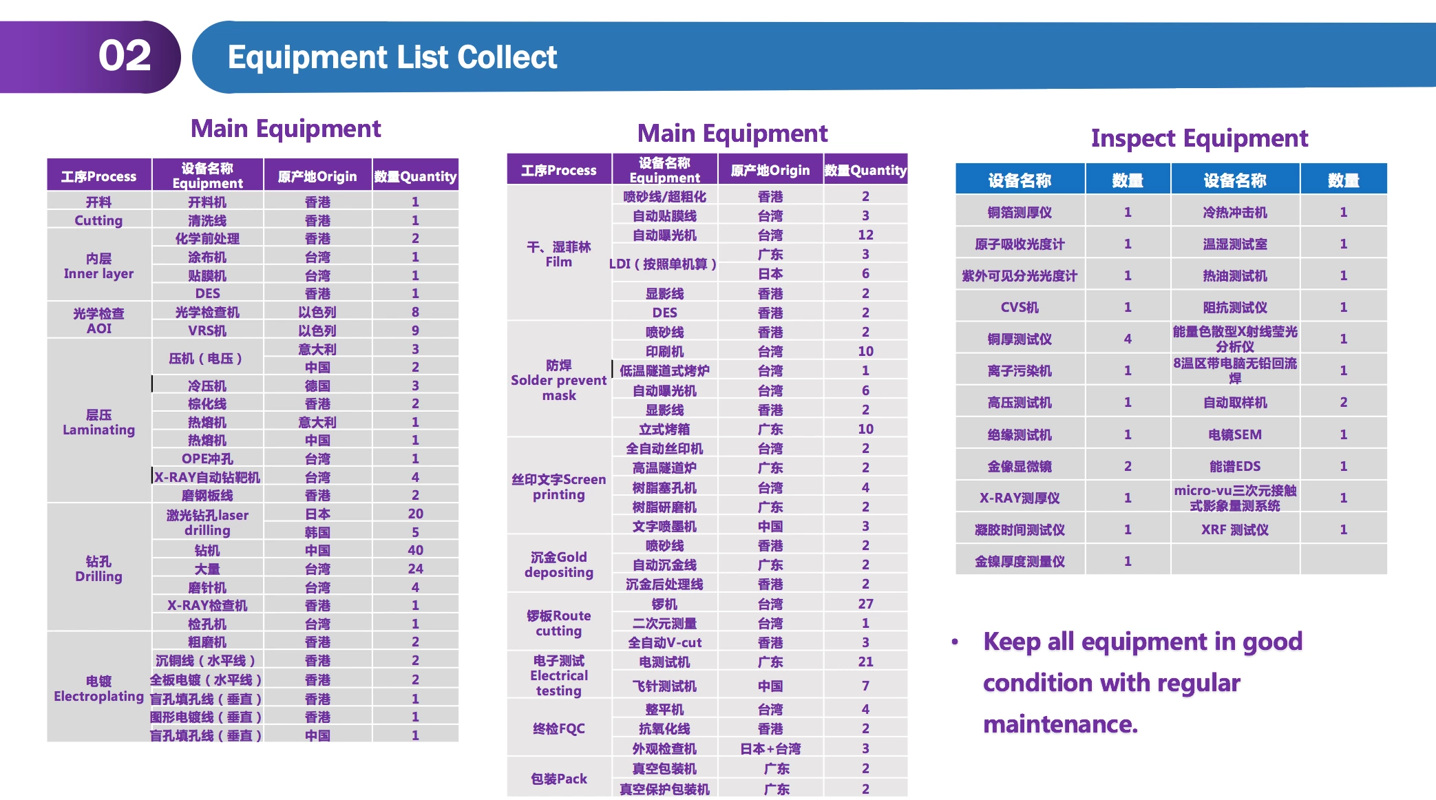
Equipment List